How to make the venerable SL1200 even better by replacing its discrete regulator with a more modern idea.
Currently under heavy review
Note
Please read the entire project, including any notes or safety warnings, before you determine if the described actions are applicable to your equipment, and that you have the required expertise and skills to implement them according to the safety laws and regulations in your area.
General Idea
The project started initially as part of an idea by Jim/6L6 from the diyaudio forum. The idea was improved with the notes of Martin from Acoustica.org.uk
Reading this will give you a nice overview of the entire project and will make the step-by-step guides easier to follow.
The entire original modification had three parts. Moving the transformer and the rectification into an external case away from the turntable, adding a CRCRC filter, and replacing the transistor-based regulator.
The first two parts are covered separately. You can read about them in the page about Technics SL1200 – PSU Modification
In this project we will cover the final part.
Replacing the regulator
The stock regulator circuit works nicely enough, however we can do better by taking advantage of more modern ideas. Jim/6L6 proposed an LM317 flavored regulator, improved by some ideas by Martin from Acoustica.org.uk
Here is the original schematic proposed
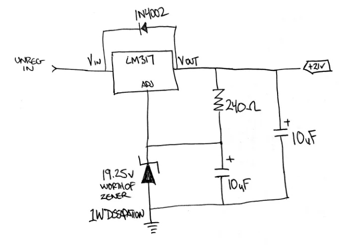
To give a rough summary, the idea is to replace the lower resistor specified in the usual datasheet schematics with a Zener diode for the voltage reference. This along with the parallel capacitor reduces the output impedance of the regulator assembly and further filters noise.
The output Voltage is defined by the Zener Voltage plus 1.25V which is the internal regulation voltage of the LM317 which develops across the resistor between the Vout and Adj pins.
Note: I do not remember if this was discussed, but this schematic will actually give closer to 20.5V output, and not 21V like the stock regulator. Refer below for more information.
Improved Implementation
Following Jim’s thread, I quickly started working on my own versions.
Below are my changes and the schematics of my current implementation (Hierarchical Kicad sheets)
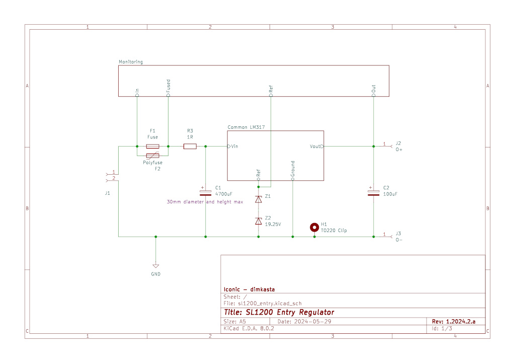
Fuse: I have added an optional fuse or pptc to protect the turntable.
Local CR stage: I have transferred the last CR stage of the proposed CRCRC filter here, so that I can use my general purpose CRC boards/projects as the main filter in the external PSU case. This has the additional benefit that it acts as a local bank, eliminating any issues caused by umbilical DC cables with high inductance, and improves transient response.
1R/3W Power Resistors: (Needs update) I have selected to use smaller power resistors than the proposed 10R/3W. I decided to do this because the 10R resistors act like a brick wall for current. There is benefit in using them though. They drop more voltage removing some thermal burden from the regulator chip. Plus, they even out the rectification ripple better. The problem is however that they also cause large voltage drops by starving the capacitor banks during transients. This was evident when starting/stopping the turntable. It caused the strobe leds to dim. And since the regulator is already very capable of eliminating low frequency ripple, I have specified a larger last capacitor. This needs some further testing.
100uF Output Capacitor: (Needs testing) This is a placeholder part. There is already an input capacitor in the turntable’s PCB (C3 and perhaps C1). I need to revisit this taking into account how the LM317 behaves with capacitive loads.
Voltage Reference: To get 21V output we actually need 19.75V worth of zener (single or multiple diodes/leds in series)
I guess the easiest is to get a 20V zener. The value is widely available, and the resulting 21.25V output is well within the normal functioning parameters of the SL1200. Later service manual versions specify 20V. Do not go much above that, because you risk frying the rare and relatively expensive ICs of the turntable.
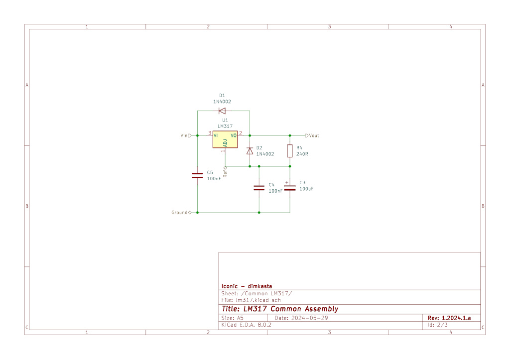
100nF bypassing capacitor: I have moved the filtering capacitor here directly in the input of the IC, since it is greatly recommended when the capacitor bank is away from the IC. It generally makes sense to use bypassing capacitors as close to the load as possible.
Reference filter capacitor (Experimental): I have added an extra 100nF capacitor next to the Zener to further filter its noise. This might mess up the output impedance of the regulator though…
Protection diode: I have also included the extra protection diode specified in the datasheet.
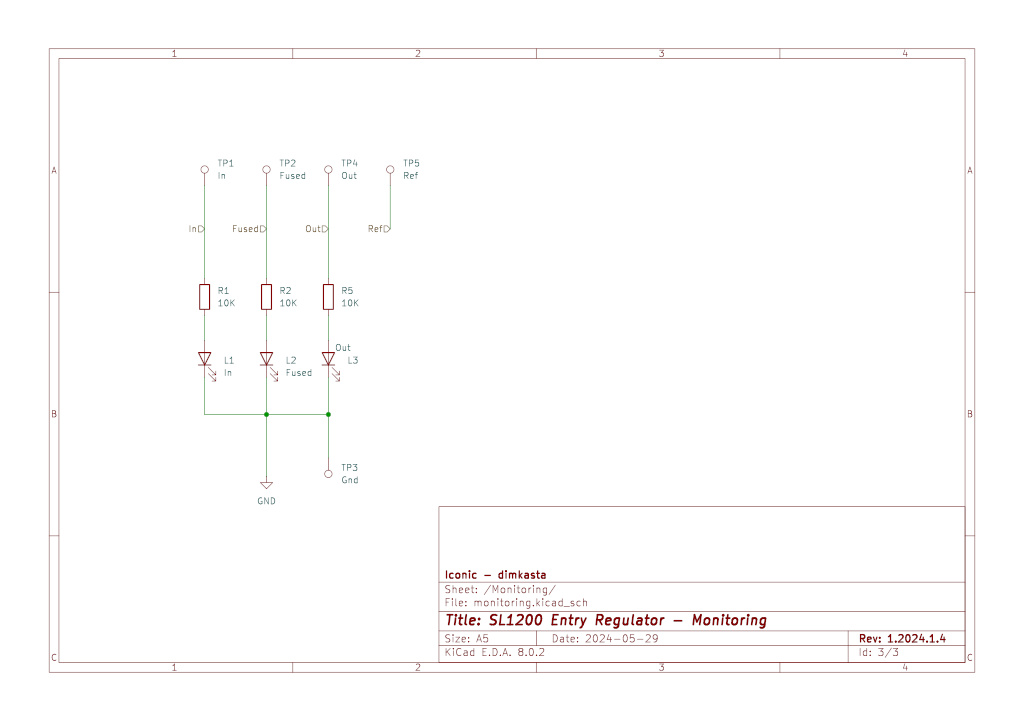
Monitoring: I have also included a few optional parts to help with monitoring and troubleshooting. That is, test points and leds for all stages of the regulator (In, fuse, Out), and a test point for the voltage reference.
TODO:
I am considering adding a TVS or a MOV to protect the ICs. I have already fried them once during my experiments by accidentally passing 31V instead of 21V.
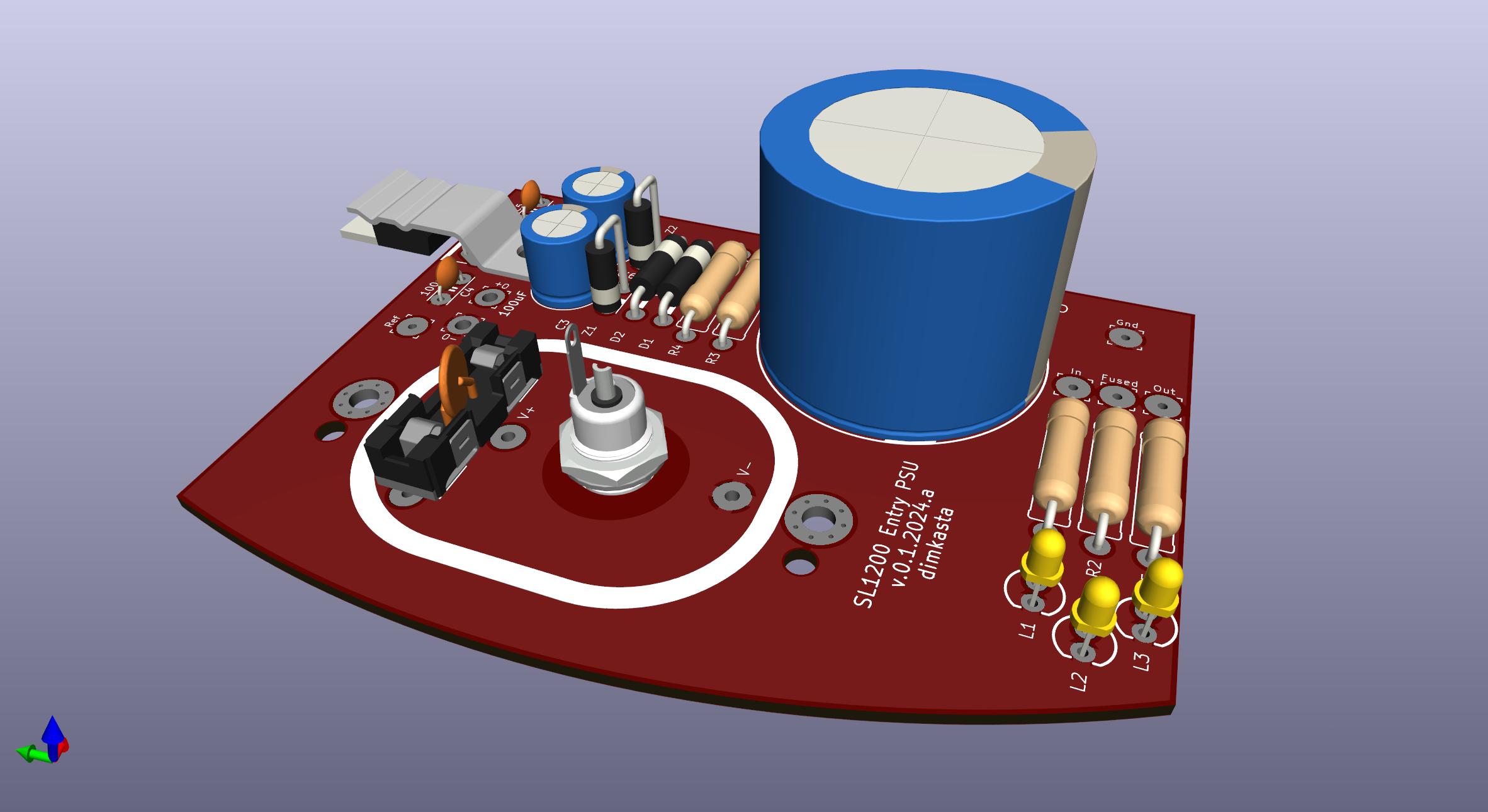
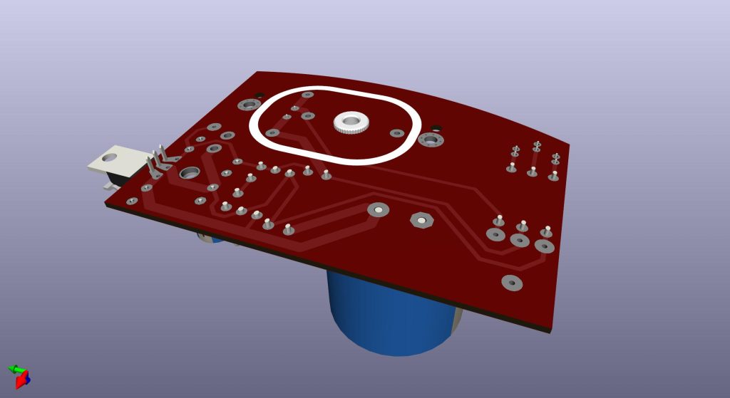
Printed Circuit Board and Implementation
The final PCB is based on my old design that fits on the bottom entry hole of the chassis. It replaces the cable entry metal part, and offers an 8mm hole for a barrel jack for the DC umbilical.
The pads are intentionally oversized. This makes them easier to solder and test, while allowing for a wide range of resistors, including RN70 or carbon composition.
The position of the platter limits the maximum height of the large capacitor to about 30mm. This is enough to give us 10000uF at 50V.
I have also added a spring clip for the TO220 chip to avoid further wear of the aluminum pad.

BOM
Here is the suggested BOM
Assembly and Installation
In this section you can see detailed instructions on how to implement this project yourself.
STOP! – Safety First
Before you put yourself or others in danger, think very carefully about whether you are qualified to carry out this work in a safe manner and in accordance to local laws and regulations
Safety is your own responsibility
Please read our Disclaimer for more information
This guide assumes that you have already removed the rectification and the filters from the turntable’s PCB, and that you have a working external PSU.
We first need to remove the existing regulation parts. The initial idea left them in place, but it’s better to remove anything that is not required.
We remove the parts D2 (D3 in some PCBs), Q1, Q2, Q3, R1, R2, R3, R4, R5, C1, and C2
We screw the assembled PCB on top of the entry point, and we make sure that the LM317 is in good thermal contact but electrically isolated from the aluminum pad. Mica pads and thermal paste should work like a charm.
The Vout is connected to entry J3, and the Ground is connected to the bottom right screw that grounds the PCB to the chassis. Or ideally to a ground point near the C3 capacitor to eliminate the effect of the inductance of the cheap one-side pcb. I chose to connect the ground to the right side of D301.
Another point that needs some attention is local bypassing.
As said above, the PCB has lots of stray inductance. And the three points of interest only have locally a 100uF capacitor. These points are the FG amplifier (circuit around Q203) and the two ICs. I chose to replace C216, C108 and C209 with a low ESR Panasonic FR capacitor at 1000uF/25V. I have had excellent results with these in local bypass duty. We might also see some improvement by adding a ceramic 100nF bypass to further eliminate high frequency noise, or add some ferrites to further isolate the 3 supplies. Ideally though, we want to separate them with their own regulator and ground. Especially the analog FG amplifier.
Suggested Parts
20V Zener 1N4747A
References:
Acoustica.org.uk – Quick Notes on using 3-pin Voltage Regulators
Technics SL1200 MK2 – Service Manual